Comprehensive Guide to Copper Oxidation States
Copper, a versatile and widely used metal, exhibits fascinating chemistry due to its multiple oxidation states. Understanding these states is…
Imagine transforming a simple piece of metal into a highly conductive, corrosion-resistant component integral to modern electronics. This is the magic of copper electroplating, a fascinating process that combines chemistry and engineering to enhance the properties of various substrates. Whether you’re looking to understand its role in semiconductor manufacturing or aiming to perfect your DIY electroplating projects, this guide dives deep into the intricate world of copper electroplating. We’ll explore the essential components of a plating bath, advanced techniques, and practical applications, all while providing solutions to common pitfalls. Ready to uncover the secrets to achieving flawless, uniform copper layers? Let’s get started.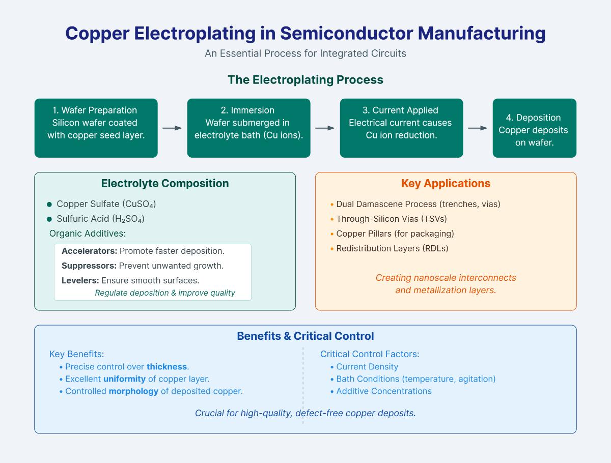
Copper electroplating is an advanced technique used to coat a conductive material with a thin, even layer of copper. This process leverages the principles of electrochemistry to achieve high-quality coatings that enhance various properties of the base material.
Copper electroplating relies on three key parts: the anode (a copper source), the cathode (the item to be plated), and the electrolyte solution. The anode is typically composed of pure copper, while the cathode is the conductive object to be plated. The electrolyte solution, usually made of copper sulfate and sulfuric acid, helps move copper ions from the anode to the cathode.
When a direct current is applied, copper ions from the anode dissolve into the electrolyte solution and migrate towards the cathode. Upon reaching the cathode, these ions gain electrons and deposit as a thin layer of copper. This continuous process results in a uniform coating, enhancing the substrate’s properties.
The anode serves as the source of copper ions. Made from pure copper, it gradually dissolves during the process, ensuring a steady supply of copper ions in the electrolyte.
The cathode is the workpiece that receives the copper coating. It must be conductive and thoroughly cleaned to ensure proper adhesion of the copper layer.
The electrolyte solution, usually a mix of copper sulfate and sulfuric acid, plays a crucial role in the electroplating process. It not only facilitates the movement of copper ions but also contains additives that control the deposition rate and quality.
A regulated direct current power supply is essential for controlling the deposition rate and ensuring uniformity in the copper layer. The current density, typically measured in amperes per square decimeter (A/dm²), is a critical parameter that influences the thickness and quality of the coating.
Before starting electroplating, the cathode’s surface needs thorough cleaning. This process includes degreasing, pickling, and sometimes sandblasting to eliminate contaminants. Ultrasonic cleaning is also used to reach complex shapes and ensure a clean surface.
The electrolyte solution is prepared by dissolving copper sulfate and sulfuric acid in water. Additives are then introduced to improve conductivity and control the deposition quality. Maintaining the optimal pH and temperature of the solution is vital to avoid defects in the plating.
The prepared anode and cathode are submerged in the electrolyte solution, ensuring they are spaced evenly to promote uniform ion distribution. The power supply is then activated, and a direct current is applied, causing copper ions to migrate from the anode to the cathode, where they deposit as a thin, uniform layer.
After reaching the desired copper thickness, the object is taken out of the electrolyte, rinsed, and dried to avoid oxidation. Further steps, like polishing, can be done to improve the copper coating’s look and performance.
Copper electroplating is widely utilized across various industries due to its ability to enhance electrical conductivity, corrosion resistance, and aesthetic appeal. In the electronics industry, it is integral to the fabrication of printed circuit boards (PCBs) and semiconductor devices. Automotive applications include coating connectors and underhood components to improve their durability. In renewable energy sectors, copper electroplating is employed in the manufacturing of solar cell electrodes and wind turbine components.
Copper electroplating involves depositing a thin copper layer onto a conductive surface using electrochemical reactions. This process immerses the substrate (cathode) and a copper anode into an electrolyte solution, typically composed of copper sulfate and sulfuric acid. An electric current is applied, causing copper ions to migrate from the anode to the cathode, forming a uniform metallic layer.
The anode, usually made from pure copper, provides copper ions. The cathode is the workpiece that receives the copper coating and must be clean and conductive. Proper surface preparation is essential, involving degreasing, pickling, and sometimes sandblasting. The electrolyte solution, typically made of copper sulfate and sulfuric acid, must be prepared and maintained at the right pH and temperature.
During the electroplating process, the prepared anode and cathode are submerged in the electrolyte solution. The power supply is then activated, and a direct current is applied, causing copper ions to migrate from the anode to the cathode. This results in the deposition of a thin, uniform layer of copper on the cathode. After achieving the desired copper thickness, the object is removed from the electrolyte, rinsed, and dried to prevent oxidation. Additional steps, such as polishing, may be performed to enhance the appearance and performance of the copper coating.
Electrolyte composition plays a significant role in the quality of the copper coating. Copper sulfate and sulfuric acid are standard components, but various additives can be used to refine plating behavior for specific geometries and applications. Current density, measured in amperes per square decimeter (A/dm²), influences the thickness and quality of the copper coating. The temperature of the electrolyte solution, typically maintained between 20–50°C, influences ion mobility and the deposition rate.
Advanced techniques include the dual damascene process for semiconductor features, TSV plating for filling vias, and creating copper pillars using photoresist-patterned substrates. The dual damascene process enables bottom-up filling for sub-100 nm semiconductor features, ensuring a uniform and defect-free copper layer. TSV plating involves filling 10–100 µm vias with copper, requiring long plating times and additives to minimize voids. Copper pillars are created using photoresist-patterned substrates and grain-refining accelerators, resulting in smooth, bright deposits essential for advanced electronic applications.
Proper surface preparation is crucial for achieving a high-quality copper electroplating finish. The workpiece, or cathode, must be meticulously cleaned to remove any contaminants that could impede the electroplating process.
The initial step involves degreasing the workpiece to eliminate oils, grease, and other organic contaminants. This can be done using solvents or alkaline cleaning solutions. Mechanical methods, such as sandblasting or abrasive brushing, can also be employed to remove stubborn residues and create a slightly roughened surface, which enhances adhesion.
After cleaning, the workpiece often undergoes an activation process. This typically involves dipping the cathode in an acid solution, such as sulfuric acid, to remove any residual oxides and increase surface reactivity. Acid activation ensures that the surface is primed for efficient copper ion deposition.
The electrolyte solution is a critical component in the copper electroplating process. It generally consists of copper sulfate and sulfuric acid, with specific additives to control deposition characteristics.
A standard industrial electrolyte bath contains copper sulfate (CuSO₄) and sulfuric acid (H₂SO₄). The copper sulfate provides the copper ions necessary for plating, while sulfuric acid enhances the solution’s conductivity and stabilizes the copper ions. Typically, the concentration for a copper sulfate bath ranges from 200 to 300 grams per liter for copper sulfate and 50 to 100 grams per liter for sulfuric acid.
Various additives can be introduced into the electrolyte to improve the quality of the copper deposit. Common additives include:
The setup for copper electroplating involves the arrangement of the anode and cathode within the electrolyte bath, along with the application of a direct current.
The workpiece (cathode) is connected to the negative terminal of the power supply, while the copper anode is connected to the positive terminal. The anode, typically made of high-purity copper, serves as the source of copper ions. Both the cathode and anode are submerged in the electrolyte solution, ensuring they are positioned correctly to promote uniform ion distribution.
A regulated direct current (DC) power supply is used to control the electroplating process. The current density, usually measured in amperes per square decimeter (A/dm²), is a critical parameter that influences the thickness and quality of the copper deposit. Typical current densities for copper electroplating range from 1 to 6 A/dm².
The actual electroplating process involves the migration of copper ions from the anode to the cathode under the influence of an electric current.
Once the setup is complete, the power supply is activated to apply a direct current. Copper ions in the electrolyte solution migrate towards the cathode. There, they gain electrons and deposit as a thin layer of copper. The deposition rate and thickness of the copper layer are controlled by adjusting the current density and the duration of the plating process.
To ensure even deposition and prevent the formation of defects such as burn spots or uneven layers, the electrolyte solution is often agitated. This can be achieved through mechanical stirring or by moving the cathode within the solution. Agitation helps maintain a uniform concentration of copper ions around the cathode surface.
After achieving the desired thickness of the copper layer, the workpiece undergoes several post-processing steps to finalize the electroplating process.
The plated workpiece is removed from the electrolyte bath and thoroughly rinsed with water to remove any residual electrolyte solution. This step is crucial to prevent corrosion and contamination.
Depending on the application, additional finishing processes may be applied to the copper-coated workpiece. These can include:
Dual damascene plating is a technique used in semiconductor manufacturing to fill etched structures on a silicon wafer with copper. This process is essential for enhancing electrical performance and miniaturizing electronic devices.
The dual damascene process involves depositing copper into etched trenches and vias on a silicon wafer. These features are patterned using photolithography and etched to form intricate pathways for electrical conduction.
Dual damascene plating is crucial in the production of sophisticated microchips, smartphones, and tablets, where it helps achieve high-density interconnections and improved device performance.
Through-silicon via plating is another advanced technique used to create 3D integrated circuits by connecting silicon wafers with copper-filled vias.
TSV plating involves filling vertical vias that pass through silicon wafers with copper, enabling the vertical stacking of wafers to increase circuit density and functionality.
TSV plating is essential for developing high-performance electronic devices that require rapid data processing and high-density packaging, such as advanced processors and memory chips.
Copper pillar plating creates reliable electrical connections in integrated circuits by forming copper pillars.
Copper pillars are formed using a patterned photoresist mask to define their locations on the substrate. This method ensures precise control over the dimensions and placement of the pillars.
Copper pillars are ideal for achieving higher density and electrical performance in integrated circuits, making them crucial for advanced electronic applications such as microprocessors and memory modules.
Redistribution layer plating involves creating an additional metal layer to redistribute electrical connections within integrated circuits.
This technique uses a thin dielectric material and a photoresist mask to pattern the redistribution layer, which is then plated with copper to form new electrical pathways.
Redistribution layer plating is used to enhance the electrical performance and reliability of integrated circuits, particularly in devices that require complex interconnections and high operational stability.
Electrolyte solutions used in copper electroplating are composed of several critical components that influence the plating quality and efficiency.
Copper sulfate is the primary salt in electroplating solutions, dissociating into copper ions that migrate to the cathode. Optimal concentration is crucial for uniform and defect-free plating.
Sulfuric acid enhances the conductivity of the electrolyte solution and suppresses hydrolysis reactions, improving the uniformity of the copper deposit.
Additives such as accelerators, suppressors, and levelers are crucial for controlling plating rates and preventing defects in complex geometries. These chemicals help achieve smooth, bright, and uniform copper layers, which are essential for high-precision applications.
Research is ongoing to develop novel additives that enhance plating efficiency and quality, particularly for filling microvias and creating complex geometries.
Efforts are being made to reduce the environmental impact of copper electroplating by optimizing electrolyte composition and improving process efficiency.
Copper electroplating is increasingly being integrated with other technologies to enhance performance in multi-layered structures and complex devices, supporting advancements in semiconductor manufacturing and electronic packaging.
Copper electroplating plays a pivotal role in the electronics and semiconductor industries, where it is used to fabricate printed circuit boards (PCBs), electrical connectors, and semiconductor devices.
In PCB manufacturing, copper electroplating is used to create conductive pathways that connect various components on the board. The process involves plating copper onto the drilled holes and surface traces, ensuring robust electrical connections and enhanced durability. Techniques like through-hole plating and surface plating are integral in achieving the desired electrical performance and reliability.
For semiconductor packaging, advanced copper electroplating techniques like dual damascene and through-silicon vias (TSV) are used to create high-density interconnections. The dual damascene process involves patterning the wafer and depositing copper in the etched regions to form intricate circuit patterns, which are essential for modern microprocessors and memory chips. TSV plating, on the other hand, enables the vertical stacking of chips by filling vias that pass through the silicon wafers with copper, thus enhancing data processing speeds and reducing power consumption.
Copper electroplating is extensively used in the automotive and aerospace sectors to improve the performance and longevity of various components.
In automotive applications, copper electroplating is used to coat connectors, terminals, and other electrical components to enhance their conductivity and resistance to corrosion. This ensures reliable performance even in harsh conditions. Additionally, copper-plated heat exchangers and radiators benefit from improved thermal conductivity, leading to better heat dissipation and engine efficiency.
In the aerospace industry, copper electroplating is applied to critical components such as electrical connectors, fasteners, and structural parts to enhance their durability and resistance to extreme temperatures and corrosion. This is vital for maintaining the safety and functionality of aerospace systems.
Copper electroplating is widely used for its aesthetic appeal and protective properties in decorative and architectural applications.
Copper electroplating is often used to enhance the appearance and durability of items such as jewelry, art pieces, and household fixtures. The warm, lustrous appearance of copper makes it a popular choice for enhancing the beauty of various decorative objects.
In architecture, copper electroplating is used to coat elements like door handles, light fixtures, and railings. The electroplated copper not only adds a sophisticated and elegant look but also provides a protective layer that prevents corrosion and wear, extending the lifespan of these features.
Copper electroplating finds applications in the medical and dental fields, where it is used to enhance the properties of various instruments and devices.
Copper-plated medical instruments benefit from improved corrosion resistance and biocompatibility, ensuring they remain sterile and functional over extended periods. This is particularly important for surgical tools and other equipment that require frequent sterilization.
In dentistry, copper electroplating is used to coat dental appliances such as braces, crowns, and bridges. The copper layer provides a strong, durable surface that resists wear and enhances the appliance’s longevity.
Copper electroplating is valuable in prototyping and rapid manufacturing. It is used to create functional prototypes and strengthen parts.
Electroplating is employed to coat 3D – printed or machined prototypes with copper, adding strength and conductivity to the parts. This is particularly useful in the early stages of product development, where functional testing of prototypes is essential.
In rapid manufacturing, copper electroplating allows for the quick production of components with enhanced mechanical and electrical properties. This technique is cost – effective and enables the efficient transition from prototype to production.
The diverse applications of copper electroplating across different industries underscore its versatility and significance in modern manufacturing and engineering.
Copper electroplating is a widely used process that often encounters various challenges. Addressing these issues effectively can significantly enhance the quality and reliability of the electroplated products.
Poor adhesion of the copper layer to the substrate can result in peeling or flaking, compromising the integrity of the coating.
Pitting and roughness on the copper surface can affect the appearance and functionality of the electroplated component.
Discoloration or dullness of the copper layer can impact both aesthetics and performance.
Inadequate coverage of the copper layer can leave parts of the substrate exposed, leading to potential corrosion and reduced effectiveness.
The presence of copper particles in the plating bath can result in rough deposits and defects.
A whitish or uneven color surface can detract from the visual appeal and indicate underlying issues with the plating process.
A rough surface can result from improper process parameters, affecting both aesthetics and performance.
Industrial copper electroplating processes use large, automated systems that allow for strict monitoring and control of various parameters. These systems are designed to handle large batches of products with consistent quality and efficiency. In contrast, DIY copper electroplating is typically conducted on a much smaller scale, often limited to individual projects or small batches. DIY setups rely on manual control, which can lead to greater variability in the results due to less precise parameter management.
The electrolyte bath used in industrial copper electroplating is formulated with a variety of special additives that control the plating process, ensuring uniform thickness, smooth finishes, and the minimization of defects. DIY copper electroplating, on the other hand, often utilizes simpler solutions such as copper sulfate and vinegar. While these solutions can achieve basic copper plating, they lack the advanced additives that enhance the quality and consistency of industrial processes.
In industrial settings, copper electroplating is used for various high-precision applications such as semiconductor manufacturing, oil and gas industry components, and electronics. For example, in semiconductor fabrication, techniques like through-silicon vias (TSVs) and dual damascene processes are employed to create intricate copper interconnects essential for modern electronic devices. The oil and gas industry uses copper electroplating to apply anti-galling coatings to critical components, enhancing their durability and performance. In electronics, copper is used to create printed circuit boards (PCBs) and redistribution layers (RDLs) that are crucial for device functionality.
DIY copper electroplating is generally used for more straightforward applications such as decorative items, small repairs, or educational projects. These applications do not require the same level of precision and control as industrial processes, making DIY methods suitable for hobbyists and small-scale users.
The quality and consistency of copper electroplating are paramount in industrial applications, where uniform thickness and defect-free coatings are essential. Industrial copper coatings are typically 0.1 to 1.2 micrometers thick and are designed to be smooth and defect-free. This level of quality is achieved through the use of advanced additives and stringent control of plating parameters.
DIY electroplating, however, often results in variable adhesion and coverage, with common issues such as bubbles or uneven layers. The lack of advanced additives and precise control in DIY setups contributes to these inconsistencies, making it challenging to achieve the same quality as industrial processes.
Setting up industrial copper electroplating is much more expensive than DIY methods. Industrial setups require specialized equipment, automated systems, and trained personnel to manage and maintain the process. This investment is justified by the high volume and stringent quality requirements of industrial applications.
DIY copper electroplating, on the other hand, is relatively low-cost, with kits available for approximately $50 to $200. These kits include basic equipment and materials necessary for small-scale plating projects. Minimal technical expertise is required to use these kits, making them accessible to hobbyists and individuals looking to explore electroplating without significant investment.
Optimizing the electrolyte chemistry in copper electroplating begins with understanding its fundamental components. The electrolyte bath typically consists of:
Alkaline copper baths include cyanide and pyrophosphate baths. While cyanide baths use copper(I) cyanide and free cyanide ions to maintain solubility, they require careful handling due to toxicity and lower current efficiency. Pyrophosphate baths are less toxic but present environmental challenges due to disposal issues.
These baths are typically used for functional plating rather than high-precision decorative or semiconductor uses.
Prepared by dissolving copper into an acetic acid/hydrogen peroxide mixture, creating copper acetate. This type of bath is suitable for small-scale or hobbyist electroplating, requiring careful control of concentration to avoid rapid, uneven deposition and poor adhesion.
In advanced copper plating, additives are critical for controlling deposit morphology and quality. They are generally categorized as:
| Additive Type | Function | Examples |
|---|---|---|
| Suppressors | Inhibit copper deposition on unwanted areas, ensuring bottom-up filling. | Polyethylene glycol (PEG), polypropylene glycol |
| Accelerators | Enhance copper deposition rate at specific locations and improve brightness. | Thiols such as 3-Mercapto-1-propanesulfonic acid, bis-(3-sodium sulfopropyl) disulfide (SPS) |
| Levelers | Control surface roughness and promote smooth, uniform deposits. | Dyes such as Janus Green B, Alcian Blue, Diazine Black |
Copper ion concentration must be balanced to ensure sufficient ion availability without causing rapid, uneven plating. In acidic baths, typical copper sulfate concentrations range from 60 to 250 g/L depending on application and current density.
Sulfuric acid enhances conductivity and plating uniformity. Too low acidity reduces conductivity, while too high acidity can increase stress in deposits.
Chloride ions are present in trace amounts (20–150 ppm) to modify deposition kinetics and improve deposit quality.
Fine-tuning suppressor, accelerator, and leveler concentrations is essential. For example, in dual damascene plating, suppressors adsorb on sidewalls, accelerators concentrate at trench bottoms, and levelers modulate top surface growth to prevent over-plating.
Typically runs near ambient to ~43°C to optimize plating rates and deposit quality.
Current density is adjusted according to bath and application, generally 1.5–20 A/dm² in acidic baths, influencing deposit thickness and morphology.
Precise control of electrolyte chemistry and additive behavior is crucial for achieving defect-free filling of nanoscale features in dual damascene and TSV processes. Accelerators promote rapid fill at the bottom of vias, suppressors prevent sidewall deposition, and levelers ensure planar top surfaces for subsequent processing.
Electrolyte additives and plating parameters are tailored to produce smooth, bright, and uniform copper features critical for interconnect reliability.
Modern electrolyte formulations favor cyanide-free acidic baths for safer handling and environmental compliance, with formulations available for hobbyists and industrial use that combine good plating quality with reduced toxicity.
| Component | Role in Electrolyte | Typical Concentration / Notes |
|---|---|---|
| Copper sulfate (CuSO₄) | Source of copper ions | 60–250 g/L (acidic baths) |
| Sulfuric acid (H₂SO₄) | Enhances conductivity and charge transfer | 45–260 g/L (acidic baths) |
| Chloride ions (Cl⁻) | Modify deposition kinetics, improve deposit quality | 20–150 ppm |
| Suppressors | Inhibit plating on unwanted areas | Polyethers (PEG, PPG) |
| Accelerators | Enhance plating rate, grain refinement | Thiols, disulfides |
| Levelers | Promote smooth, uniform surface | Organic dyes |
| pH | Maintained acidic (~0.5–1.5) in acid baths, alkaline in cyanide baths | Critical for deposition quality |
| Temperature | Controls plating rate and deposit properties | Ambient to ~43°C |
| Current density | Influences thickness, grain size, plating speed | 1.5–20 A/dm² (acidic baths) |
Optimizing these parameters ensures superior plating quality, improved reliability, and tailored material properties aligned with specific technological demands.
In the electronics industry, copper electroplating is critical for manufacturing components like printed circuit boards (PCBs) and semiconductor devices. Following industry-specific best practices ensures high-quality and reliable outcomes.
In the automotive industry, copper electroplating enhances the performance and longevity of electrical and mechanical components.
In aerospace applications, copper electroplating is used to protect critical components from extreme conditions.
Copper electroplating in the medical field enhances the functionality and longevity of instruments and devices.
Copper electroplating is widely used for its aesthetic appeal in decorative and architectural applications.
Below are answers to some frequently asked questions:
Copper electroplating in semiconductor manufacturing is an essential process for creating copper interconnects and metallization layers in integrated circuits. The technique involves submerging a silicon wafer, which is coated with a thin copper seed layer, into an electrolyte bath containing copper ions. An electrical current is then applied, causing copper ions to be reduced and deposited onto the wafer surface.
This process ensures precise control over the thickness, uniformity, and morphology of the copper layer. The electrolyte typically consists of copper sulfate and sulfuric acid, along with organic additives that regulate deposition rates and improve the quality of the plated copper. Accelerators promote faster copper deposition at specific regions, suppressors prevent unwanted growth, and levelers ensure smooth surfaces.
Key applications in semiconductor manufacturing include the dual damascene process for creating nanoscale trenches and vias, through-silicon vias (TSVs), copper pillars for packaging, and redistribution layers (RDLs). Proper control of current density, bath conditions, and additive concentrations is crucial to achieving high-quality, defect-free copper deposits.
The key components of a copper electroplating bath are essential for achieving effective copper deposition. The primary components include:
Together, these components create a balanced chemical environment that ensures efficient and uniform copper deposition, critical for applications such as semiconductor packaging and electronic contacts.
To avoid defects during DIY copper electroplating, start with thorough surface preparation. Clean the metal surface using a degreaser or specialized cleaner to remove oils, dirt, and oxidation, and for stubborn residues, use a diluted hydrochloric acid etch. Always handle parts with gloves to prevent contamination. Maintain a clean and balanced electrolyte bath by using pure copper anodes, regularly filtering the solution, controlling bath composition, and avoiding contamination. Control electrical parameters, ensuring correct polarity, using low and stable current density, maintaining proper distance between anode and cathode, and agitating the object during plating. Prevent common defects by addressing their causes, such as using a nickel strike layer for poor adhesion or regular filtering for pitting. After plating, rinse the object thoroughly, protect it from oxidation, and avoid rough polishing. Additionally, use gloves, keep the solution at a suitable temperature, ensure good electrical contact, and adjust amperage during long runs.
Achieving uniform copper electroplating requires adherence to several best practices that ensure the final product’s quality and consistency. Start with thorough surface preparation, including cleaning with alkaline cleaners and acid dips to remove contaminants, and polishing to smoothen the surface. Maintain proper control of the electrolyte bath by ensuring the optimal concentration of copper ions, typically using copper sulfate, and monitoring the pH to keep it between 0.5 and 1.5. Additives like brighteners can enhance the finish.
Consistent process conditions are crucial, including applying a steady current density (1-5 A/dm²) and voltage (1-3 V), and maintaining a stable temperature (20-40°C) with gentle agitation to avoid uneven deposits. Regularly replace copper anodes to ensure a steady supply of copper ions. Moving the object during plating can prevent localized accumulation of copper, known as “burn spots,” ensuring even adhesion.
Post-plating, rinse and dry the object thoroughly to remove residual solution and prevent corrosion. Optionally, polish or apply a protective clear coat to maintain the finish. Following these practices will help achieve high-quality, uniform copper electroplating suitable for various applications.
Plating additives play a crucial role in determining the quality of electroplated copper. These additives, categorized into accelerators, inhibitors, levelers, and suppressors, each serve specific functions to enhance the electroplating process.
Accelerators like sodium propylsulfonate (SPS) and methyl propylsulfonate (MPS) increase the deposition rate of copper ions, resulting in a bright and uniform finish. Inhibitors such as polyethylene glycol (PEG) slow down the deposition rate, helping to achieve a uniform coating, especially on complex geometries. Levelers, often dye-based or non-dye-based, ensure a smooth surface finish by preventing excessive copper buildup on protrusions. Suppressors, commonly polyalkyl glycols, maintain a uniformly wetted surface, contributing to a stable plating process.
These additives collectively improve the uniformity, brightness, surface smoothness, adhesion, and durability of the electroplated copper. They also influence the microstructure, affecting properties like electrical conductivity. Proper selection and dosing of additives are essential for optimal electroplating results.
The main differences between industrial and DIY copper electroplating lie in process control, bath composition, substrate preparation, application scope, quality and consistency, safety, and cost.
Industrial copper electroplating involves tightly controlled parameters, advanced equipment, and specialized electrolyte formulations. This ensures uniform deposition, high precision, and the ability to handle complex geometries. Rigorous substrate preparation and proprietary additives enhance adhesion and minimize defects. Industrial applications target functional outcomes in sectors like aerospace and electronics, adhering to strict safety regulations and achieving high repeatability.
In contrast, DIY copper electroplating relies on basic tools and simplified solutions, resulting in inconsistent current distribution and coarse-grained deposits. Manual cleaning methods often lead to poor bonding and increased defects. DIY projects are typically small-scale and cosmetic, with limited structural reliability. Safety protocols are often overlooked, increasing exposure risks. While DIY methods are cost-effective for small batches, they are impractical for mass production or high-precision requirements.

